- 您现在的位置:买卖IC网 > Sheet目录2008 > MAX1197ECM+TD (Maxim Integrated Products)IC ADC 8BIT 60MSPS DL 48-TQFP
MAX1197
Dual, 8-Bit, 60Msps, 3V, Low-Power ADC with
Internal Reference and Parallel Outputs
4
_______________________________________________________________________________________
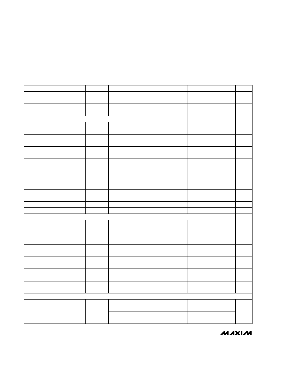
ELECTRICAL CHARACTERISTICS (continued)
(VDD = OVDD = 3V, 0.1F and 2.2F capacitors from REFP, REFN, and COM to GND; REFOUT connected to REFIN through a 10k
resistor, VIN = 2VP-P (differential with respect to COM), CL = 10pF at digital outputs, fCLK = 60MHz, TA = TMIN to TMAX, unless otherwise
noted.
≥ +25°C guaranteed by production test, < +25°C guaranteed by design and characterization. Typical values are at TA = +25°C.)
PARAMETER
SYMBOL
CONDITIONS
MIN
TYP
MAX
UNITS
Differential Reference Output
Voltage Range
VREF
VREF = VREFP - VREFN
1.024
±3%
V
Reference Temperature
Coefficient
TCREF
±100
ppm/°C
BUFFERED EXTERNAL REFERENCE (VREFIN = 2.048V)
Positive Reference Output
Voltage
VREFP
(Note 5)
2.012
V
Negative Reference Output
Voltage
VREFN
(Note 5)
0.988
V
Common-Mode Level
VCOM
(Note 5)
VDD / 2
±0.1
V
Differential Reference Output
Voltage Range
VREF
VREF = VREFP - VREFN
1.024
±2%
V
REFIN Resistance
RREFIN
750
M
Maximum REFP, COM Source
Current
ISOURCE
5mA
Maximum REFP, COM Sink
Current
ISINK
-250
A
Maximum REFN Source Current
ISOURCE
250
A
Maximum REFN Sink Current
ISINK
-5mA
UNBUFFERED EXTERNAL REFERENCE (VREFIN = AGND, reference voltage applied to REFP, REFN, and COM)
REFP, REFN Input Resistance
RREFP,
RREFN
Measured between REFP, COM, REFN,
and COM
4k
REFP, REFN, COM Input
Capacitance
CIN
15
pF
Differential Reference Input
Voltage Range
VREF
VREF = VREFP - VREFN
1.024
±10%
V
COM Input Voltage Range
VCOM
VDD / 2
±5%
V
REFP Input Voltage
VREFP
VCOM +
VREF / 2
V
REFN Input Voltage
VREFN
VCOM -
VREF / 2
V
DIGITAL INPUTS (CLK, PD,
OE, SLEEP, T/B)
CLK
0.8
×
VDD
Input High Threshold
VIH
PD,
OE, SLEEP, T/B
0.8
×
OVDD
V
发布紧急采购,3分钟左右您将得到回复。
相关PDF资料
MAX1202AEPP+
IC ADC 12BIT 8CH 20-DIP
MAX121EAP+
IC ADC 14BIT 308KSPS 20SSOP
MAX1238MEEE+T
IC ADC 12BIT SERIAL 16-QSOP
MAX1240AEPA+
IC ADC 12BIT SERIAL 8-DIP
MAX1245BCPP
IC ADC SRL 12BIT 2.375V 20-DIP
MAX1249AEPE+
IC ADC 10BIT SERIAL 16-DIP
MAX1279AETC+
IC ADC 12BIT 1.5MSPS 12-TQFN
MAX1285BESA+T
IC ADC 12BIT 300KSPS 8-SOIC
相关代理商/技术参数
MAX1197ECM-D
功能描述:模数转换器 - ADC RoHS:否 制造商:Texas Instruments 通道数量:2 结构:Sigma-Delta 转换速率:125 SPs to 8 KSPs 分辨率:24 bit 输入类型:Differential 信噪比:107 dB 接口类型:SPI 工作电源电压:1.7 V to 3.6 V, 2.7 V to 5.25 V 最大工作温度:+ 85 C 安装风格:SMD/SMT 封装 / 箱体:VQFN-32
MAX1197ECM-TD
功能描述:模数转换器 - ADC RoHS:否 制造商:Texas Instruments 通道数量:2 结构:Sigma-Delta 转换速率:125 SPs to 8 KSPs 分辨率:24 bit 输入类型:Differential 信噪比:107 dB 接口类型:SPI 工作电源电压:1.7 V to 3.6 V, 2.7 V to 5.25 V 最大工作温度:+ 85 C 安装风格:SMD/SMT 封装 / 箱体:VQFN-32
MAX1198E/D
功能描述:模数转换器 - ADC DICE SALES DICE RoHS:否 制造商:Texas Instruments 通道数量:2 结构:Sigma-Delta 转换速率:125 SPs to 8 KSPs 分辨率:24 bit 输入类型:Differential 信噪比:107 dB 接口类型:SPI 工作电源电压:1.7 V to 3.6 V, 2.7 V to 5.25 V 最大工作温度:+ 85 C 安装风格:SMD/SMT 封装 / 箱体:VQFN-32
MAX1198ECM+D
功能描述:模数转换器 - ADC 8-Bit 2Ch 100Msps 3.3V High Speed ADC RoHS:否 制造商:Texas Instruments 通道数量:2 结构:Sigma-Delta 转换速率:125 SPs to 8 KSPs 分辨率:24 bit 输入类型:Differential 信噪比:107 dB 接口类型:SPI 工作电源电压:1.7 V to 3.6 V, 2.7 V to 5.25 V 最大工作温度:+ 85 C 安装风格:SMD/SMT 封装 / 箱体:VQFN-32
MAX1198ECM+TD
功能描述:模数转换器 - ADC 8-Bit 2Ch 100Msps 3.3V High Speed ADC RoHS:否 制造商:Texas Instruments 通道数量:2 结构:Sigma-Delta 转换速率:125 SPs to 8 KSPs 分辨率:24 bit 输入类型:Differential 信噪比:107 dB 接口类型:SPI 工作电源电压:1.7 V to 3.6 V, 2.7 V to 5.25 V 最大工作温度:+ 85 C 安装风格:SMD/SMT 封装 / 箱体:VQFN-32
MAX1198ECM-D
功能描述:模数转换器 - ADC RoHS:否 制造商:Texas Instruments 通道数量:2 结构:Sigma-Delta 转换速率:125 SPs to 8 KSPs 分辨率:24 bit 输入类型:Differential 信噪比:107 dB 接口类型:SPI 工作电源电压:1.7 V to 3.6 V, 2.7 V to 5.25 V 最大工作温度:+ 85 C 安装风格:SMD/SMT 封装 / 箱体:VQFN-32
MAX1198ECM-TD
功能描述:模数转换器 - ADC RoHS:否 制造商:Texas Instruments 通道数量:2 结构:Sigma-Delta 转换速率:125 SPs to 8 KSPs 分辨率:24 bit 输入类型:Differential 信噪比:107 dB 接口类型:SPI 工作电源电压:1.7 V to 3.6 V, 2.7 V to 5.25 V 最大工作温度:+ 85 C 安装风格:SMD/SMT 封装 / 箱体:VQFN-32
MAX1198EVKIT
功能描述:数据转换 IC 开发工具 RoHS:否 制造商:Texas Instruments 产品:Demonstration Kits 类型:ADC 工具用于评估:ADS130E08 接口类型:SPI 工作电源电压:- 6 V to + 6 V